| |
| The worthiness of a field
of study or the benefit of combining technologies -- such as the integration
of nanoscience and biotechnology -- becomes most apparent when engineers
explore how it can be applied across many disciplines to improve the
quality of life. |
In the first volume of
his journal The Writings of Henry David Thoreau, in the letter describing “A
Week on the Concord and Merrimack Rivers,” the philosopher, author,
and naturalist said, “The newest is but the oldest made visible
to our senses.” His reflection is as true now as it was in 1849.
People perceive truth from what they see, and from what they cannot
see they extrapolate, reason, trust, or fabricate. When they are finally
able to visualize an item or idea, it is not necessarily “new.” More
than likely it was there all along. Perhaps this is why researchers
continually look for ways to see beyond the immediately visible. They
explore, observe, and record the “invisible,” so that they
can better understand what they are able to see and then begin to use
that knowledge.
 Such is the case with the nano- and biosensor research
being conducted at the University of Notre Dame, as some of the “invisibles” that
faculty in the College of Engineering have been exploring involve activities
on the nano scale. Nanotechnology describes the process of creating
new structures or systems atom by atom. It focuses on materials whose
components exhibit novel properties -- physical, chemical, and
biological -- due to their size: from a single nanometer to 100
nanometers. And, its potential is enormous. According to the June 2004
issue of Physics Today, “Scientists
predict that applications of nanotechnology will go far beyond their current
uses -- in sunblock, stain-resistant clothing, and catalysts -- to,
for example, environmental remediation, power transmission, and disease diagnosis
and treatment.” Because researchers and investors continue to envision
a world with molecule-sized clot-breaking machines and drug-delivery devices,
the annual worldwide investment in nanotechnology has exceeded $3.5 billion. Such is the case with the nano- and biosensor research
being conducted at the University of Notre Dame, as some of the “invisibles” that
faculty in the College of Engineering have been exploring involve activities
on the nano scale. Nanotechnology describes the process of creating
new structures or systems atom by atom. It focuses on materials whose
components exhibit novel properties -- physical, chemical, and
biological -- due to their size: from a single nanometer to 100
nanometers. And, its potential is enormous. According to the June 2004
issue of Physics Today, “Scientists
predict that applications of nanotechnology will go far beyond their current
uses -- in sunblock, stain-resistant clothing, and catalysts -- to,
for example, environmental remediation, power transmission, and disease diagnosis
and treatment.” Because researchers and investors continue to envision
a world with molecule-sized clot-breaking machines and drug-delivery devices,
the annual worldwide investment in nanotechnology has exceeded $3.5 billion.
Another “invisible” that’s gained impetus in the
last few years is biotechnology, which uses living organisms and their
by-products to develop or improve plants, animals, and products for
specific purposes. Early “biotechnology” included plant
and animal breeding techniques and the use of yeast in making beer,
bread, and wine. Today, biotechnology includes manipulating genes to
tailor new types of living cells for emerging environmental and industrial
needs.
 Researchers suggest that the potential of the interface of these
two key technologies, which has proven to be truly multidisciplinary,
lies in the fact that nanotechnology operates at the same level --
the molecular or subcellular scale -- as biological processes. This
new field, which some call nanobiotechnology, integrates elements of
nanotechnology and biotechnology in order to develop
solutions for some of the problems facing society today, including
challenges in the medical, information technology, security, and aerospace
industries, as well as in environmental protection. Researchers suggest that the potential of the interface of these
two key technologies, which has proven to be truly multidisciplinary,
lies in the fact that nanotechnology operates at the same level --
the molecular or subcellular scale -- as biological processes. This
new field, which some call nanobiotechnology, integrates elements of
nanotechnology and biotechnology in order to develop
solutions for some of the problems facing society today, including
challenges in the medical, information technology, security, and aerospace
industries, as well as in environmental protection.
|
 |
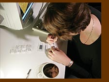
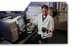
One of the hottest topics
in nanobiotechnology is its potential for medical applications, especially
in the areas of drug delivery and diagnostic devices. Agnes
E. Ostafin, assistant professor of chemical and biomolecular engineering, believes that
living cells themselves may provide the best clues for developing materials
suitable for use as biosensors or drug-delivery vehicles. “One of the
projects we’ve been working
on,” she says, “involves red blood cells.” These cells are
attractive for research because they have a specific function: They transport
oxygen through capillaries to cells. To do this, they have to be flexible enough
to change shape, fitting within different sized capillaries as they travel
through the body.
 According to Ostafin, the red blood cells of diabetics or
people with sickle cell anemia are unusually rigid. They can’t bend or change
their shape easily, which can lead to blood clots or strokes. “In
our studies,” she says, “we’ve been paying special
attention to the proteins within cells. What gives some cells their
shape -- red blood
cells in this case -- is a meshwork of proteins.” Ostafin explains
that this meshwork responds differently to different biochemical signals. Under
certain circumstances, the mesh opens, allowing interaction with the triggering
chemical. At other times, the mesh remains closed. According to Ostafin, the red blood cells of diabetics or
people with sickle cell anemia are unusually rigid. They can’t bend or change
their shape easily, which can lead to blood clots or strokes. “In
our studies,” she says, “we’ve been paying special
attention to the proteins within cells. What gives some cells their
shape -- red blood
cells in this case -- is a meshwork of proteins.” Ostafin explains
that this meshwork responds differently to different biochemical signals. Under
certain circumstances, the mesh opens, allowing interaction with the triggering
chemical. At other times, the mesh remains closed.
“Once we understand the situations which make this mesh open
and close,” says Ostafin, “we can begin to apply that knowledge
to create synthetic meshes. Or perhaps we could deliver a drug that
would help a cell regulate its sensing of chemicals, so it would begin
to function more normally. We could develop synthetic cells (or bags)
that could carry a drug to a selected site in the body and then, using
the concept of opening and closing the meshwork, design it to interact
with the chemical conditions of a specific disease. These are all possibilities,
but first we must understand the physical biochemical reactions that
are taking place.”
Another project directed by Ostafin involves the self-assembly of
nanoshells. These shells, whose hollow cores are approximately 100
nanometers in diameter (the size of one human gene), are so small that
they do not behave as expected: Semiconductor materials a few nanometers
large begin to emit light, metals become catalytic, and interfacial
chemistry dominates kinetics and particle dynamics. “Our goal
is to find out how we can learn to control molecular assembly,” says
Ostafin, “to make a molecule brighter or to control a chemical
reaction, possibly preserving it within a solvent-filled core -- so
it occurs more efficiently.”
Ostafin and her team have many questions to answer, but the first
step, she contends, always involves basic studies. Working with several
graduate and undergraduate students, Ostafin has shown that dye molecules
placed inside nanoshells glow brightly. “We’ve been working on
this project for some time and have developed many different recipes to make
a variety of particles,” she says. “We believe they could prove
to be useful mobile sensors, perhaps even tracking cancer in the body.”
 According to Ostafin, coating the outer surface of the nanoshells
with other chemicals helps the structures evade the body’s immune
system while targeting specific tissues. “Once
the shells have attached to the target,” she says, “they ‘glow,’ making
the targeted molecule or cell much easier to see for diagnostic purposes.
At that point we can consider tailoring the disassembly of the nanoshells,
so that they can either deliver a therapeutic payload to the site or signal
physicians when the biochemical environment near the targeted tissue is abnormal.
This additional information would improve a physician’s ability to
design a treatment regime or track a patient’s progress.” According to Ostafin, coating the outer surface of the nanoshells
with other chemicals helps the structures evade the body’s immune
system while targeting specific tissues. “Once
the shells have attached to the target,” she says, “they ‘glow,’ making
the targeted molecule or cell much easier to see for diagnostic purposes.
At that point we can consider tailoring the disassembly of the nanoshells,
so that they can either deliver a therapeutic payload to the site or signal
physicians when the biochemical environment near the targeted tissue is abnormal.
This additional information would improve a physician’s ability to
design a treatment regime or track a patient’s progress.”
Ostafin stresses that her team is not developing “a cure for
cancer,” although she is excited about the potential medical
applications of this research. “The most important thing to remember
about the nano- and bioengineering efforts at Notre Dame is that there’s
scientific merit in the work that’s occurring throughout the
college,” she says. “When we understand a system, and why
and how it works, that’s when we’ve really opened the door
for discovery and innovation.”
In fact, a basic understanding
of biotechnology is the focus of a laboratory course elective for seniors
that Ostafin will be introducing this fall within the Department of
Chemical and Biomolecular Engineering. Ostafin believes the lab experience
will give students hands-on opportunities to use the tools of biotechnology,
allowing them to contribute more meaningfully to this growing field.
For more information on Ostafin's research, visit www.nd.edu/~aostafin.
|
The
Center for Nano Science and Technology
 Nanoscience research was not
new to the College of Engineering when the Center for Nano Science
and Technology was established in 1999. In fact, the creation of the
center culminated 15 years of faculty research and development in this
area. Led by the Department of Electrical Engineering since its inception,
the center continues to explore the fundamental concepts of nanoscience
in order to develop unique engineering applications. It integrates
research in biological, molecular, and semiconductor-based nano-structures;
device concepts and modeling; nanofabrication and characterization;
and information processing architectures and design. Nanoscience research was not
new to the College of Engineering when the Center for Nano Science
and Technology was established in 1999. In fact, the creation of the
center culminated 15 years of faculty research and development in this
area. Led by the Department of Electrical Engineering since its inception,
the center continues to explore the fundamental concepts of nanoscience
in order to develop unique engineering applications. It integrates
research in biological, molecular, and semiconductor-based nano-structures;
device concepts and modeling; nanofabrication and characterization;
and information processing architectures and design.
Activities in the
center include multidisciplinary projects in Quantum-dot Cellular Automata,
a paradigm for transistorless computing pioneered at the University;
resonant-tunneling devices and circuits; photonic integrated circuits;
quantum transport and hot carrier effects in nanodevices; optical and
high-speed nano-based materials, devices, and circuits; the role of
non-equilibrium thermodynamics in influencing the properties of nanodevices;
and the interaction of biological systems with semiconductors.
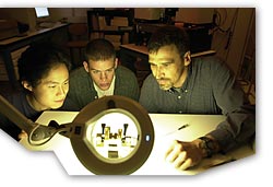
“One of the
current projects,” says Wolfgang Porod, center
director and Freimann Professor of Electrical Engineering, “focuses
on developing a new generation of parallel processing chips that can
capture both visible and invisible -- infrared -- light. It’s
very exciting because we’re using the mammalian retina, specifically
the way the sensors in an eye are connected, as a model for the vision
sensors which will be placed on these chips.”
The project is one
of only 16 to have received a grant in 2003 from the Multidisciplinary
University Research Initiative (MURI) program. Sponsored by the Department
of Defense, the MURI program is designed to encourage the development
of multidisciplinary teams from several universities whose efforts
address more than one traditional science and engineering discipline
critical to national defense. Partnering with the University’s
Center for Nano Science and Technology on the MURI project are the
Vision Research Laboratory and the Nonlinear Electronics Laboratory
of the University of California at Berkeley, the Molecular Vision Laboratory
at Harvard University, the Signal Processing System Design Laboratory at Notre
Dame, and Pazmany Peter Catholic University in Budapest, Hungary.
Porod and the MURI
team are clear; they are not “inventing” a parallel processing
chip. “That’s been done,” says Porod. “By employing
the concept of cellular neural/nonlinear networks, image acquisition
and data processing on the same chip at the same time has already been
accomplished by researchers other than those at Notre Dame. The challenge
with the most recent generation of parallel processing chips, and the
problem we are addressing, is that it is difficult for the current
chips to ‘see’ different colors at
high speeds. Another concern is that they can’t detect infrared light,
which is useful in a variety of applications.”
According to Yih-Fang
Huang, professor and chair of the Department of Electrical Engineering,
a number
of systems -- including target detection, navigation, tracking, and robotics
-- rely upon information beyond the visible spectrum, such as ultraviolet rays,
infrared rays, and radio waves. “The military certainly has a great interest
in detecting infrared light,” says Huang, “but there are many civilian
uses for this research as well, including law enforcement and medical applications.”
The team describes
the project as an example of the convergence of nanotechnology, biotechnology,
and information technology, but it is more importantly a project designed
to solve a vision problem: developing sensors for parallel processing
chips that will detect infrared light, which is why the team is modeling
the connections within the eye.
 A mammalian retina
contains millions of light-sensitive cells called rods and cones. Rods
are sensitive to dim light but cannot distinguish wavelengths. Cones
come in three types, which respond to short, middle, and long wavelengths,
respectively. All of the cones are used to capture light, after which
electrical signals are sent to the brain, where they are organized
and interpreted as images. “Obviously, the eye cannot sense infrared
light,” says Patrick J. Fay, associate professor of electrical
engineering, “but because of the way it works, it makes great
sense to use the eye as a model for the development of vision chips
with nanoscale multispectral sensors.” A mammalian retina
contains millions of light-sensitive cells called rods and cones. Rods
are sensitive to dim light but cannot distinguish wavelengths. Cones
come in three types, which respond to short, middle, and long wavelengths,
respectively. All of the cones are used to capture light, after which
electrical signals are sent to the brain, where they are organized
and interpreted as images. “Obviously, the eye cannot sense infrared
light,” says Patrick J. Fay, associate professor of electrical
engineering, “but because of the way it works, it makes great
sense to use the eye as a model for the development of vision chips
with nanoscale multispectral sensors.”
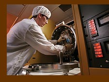
“Using nanotechnologies
such as electron beam lithography, atomic force microscopy, and scanning-tunneling
microscopy,” says Gary H. Bernstein, “we
can fabricate these bio-inspired sensors so that they function comparably
to the cones in a retina.” Then the sensors, tens of thousands
of nanoscale antennae, will be placed on a silicon chip to assist in
the acquisition and processing of infrared images.
A multidisciplinary effort, the Center for Nano Science and Technology
brings together faculty from many departments across campus. They include:
Department of Electrical Engineering
Gary H. Bernstein, professor
Arpad Csurgay, visiting faculty
Patrick J. Fay, associate professor
Douglas C. Hall, associate professor
Debdeep Jena, assistant professor
Thomas H. Kosel, associate professor
Craig S. Lent, professor
James L. Merz, professor
Alexander Mintairov, research faculty
Alexei Orlov, research faculty
Wolfgang Porod, center director and Freimann
Professor
Alan C. Seabaugh, associate director of the center and professor
Gregory
L. Snider, associate professor
Huili (Grace) Xing, assistant professor
Department of Chemical and Biomolecular Engineering
Agnes E. Ostafin,
assistant professor
Department of Chemistry and Biochemistry
Thomas P. Fehlner, Grace-Rupley
Professor
Holly V. Goodson, assistant professor
Gregory V. Hartland, associate professor
Paul W. Huber, professor
Marya Lieberman, associate professor
Olaf Wiest, associate professor
Department of Computer Science and Engineering
Jay B. Brockman, associate
professor
Jesus A. Izaguirre, assistant professor
Peter M. Kogge, Ted H. McCourtney
Professor
Department of Physics
Malgorzata Dobrowolska-Furdyna, professor
Jacek Furdyna, professor
Boldizsar Janko, assistant professor
For more information on the center,
its facilities, personnel, and research initiatives, visit www.nd.edu/~ndnano.
|
 |
 Although hundreds of
security efforts have risen in the wake of 9-11, this particular project
of Alan C. Seabaugh, professor of electrical engineering and associate
director of the Center for Nano Science and Technology, began with
a call for proposals in 1999, when the United Engineering Foundation
requested papers on the development of anti-terrorist technology. Seabaugh’s
idea was one of the four selected from a total of 920 proposals. His
concept focused on the creation of a handheld biotoxin analyzer that
could be used at potentially contaminated sites, such as the aftermath
of a terrorist attack or an industrial accident. Although hundreds of
security efforts have risen in the wake of 9-11, this particular project
of Alan C. Seabaugh, professor of electrical engineering and associate
director of the Center for Nano Science and Technology, began with
a call for proposals in 1999, when the United Engineering Foundation
requested papers on the development of anti-terrorist technology. Seabaugh’s
idea was one of the four selected from a total of 920 proposals. His
concept focused on the creation of a handheld biotoxin analyzer that
could be used at potentially contaminated sites, such as the aftermath
of a terrorist attack or an industrial accident.
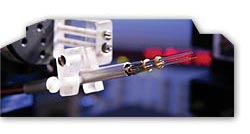
Instead of using a
light source to illuminate a toxin, which is a traditional way of “seeing” dangerous substances, Seabaugh’s
expertise in nanoelectronics led him to suggest using microwave reflection.
The use of microwaves would provide the same accurate measurements
as the typical optical method but allow the finished device to be much
smaller than other devices, possibly the size of a credit card.
Working
with graduate students Wei Zhao, Srivatsan
Srinivasan, and Qing Liu, Seabaugh designed a semiconductor chip that featured micromachined
silicon waveguides through which fluids would travel. The same channels
that conducted the fluid would guide the electromagnetic waves.
Completing
the requirements for the original proposal in June 2004, Seabaugh and
his team demonstrated a prototype of the concept. “The next
step ... whether planning to use this device as an attack detector or
as a medical diagnostic device,” says Seabaugh, “is to develop
microwave tags for specific toxins or chemicals and create a database
on the chip for each of those toxins. This type of device could eventually assist
in the safe and targeted deployment of personnel and resources to specific
sites with detailed information about the type and level of toxin involved.
It could make emergency efforts much more effective.”
For more information on the biotoxin analyzer, visit www.nd.edu/~nano/projects/chembio.html.
|
 |
Aerospace engineers track
the wind and measure its velocity as it whips through cities. In today’s
environment, city officials and emergency teams also need this type
of information ... to predict the path of pollutants and assess their
toxicity.
An ultrasonic anemometer is a device that is currently used
to provide three-dimensional wind measurements. But the anemometers
available today are too large to obtain the small-scale measurements
of velocity and temperature that would be required for many fluid dynamics
and security applications. For this reason Scott
C. Morris, assistant
professor of aerospace and mechanical engineering, is developing the
first microsonic anemometer.
 Morris’ microsonic anemometer, proposed to be less than 1/30
the size of current devices, will record turbulent flows with up to
60 times the resolution of other anemometers. This will provide better
information for the modeling of air flows and chemical dispersion throughout
a city. “For example,” says Morris, “a chemical detector
on a roof top may alert officials to danger, but alone it cannot provide
information on where a toxin came from or predict where it’s
going. The effective modeling of cityscapes, using the information
provided by a series of microsonic anemometers, would offer the predictive
capability necessary to ensure the safety of a city’s inhabitants.” Morris’ microsonic anemometer, proposed to be less than 1/30
the size of current devices, will record turbulent flows with up to
60 times the resolution of other anemometers. This will provide better
information for the modeling of air flows and chemical dispersion throughout
a city. “For example,” says Morris, “a chemical detector
on a roof top may alert officials to danger, but alone it cannot provide
information on where a toxin came from or predict where it’s
going. The effective modeling of cityscapes, using the information
provided by a series of microsonic anemometers, would offer the predictive
capability necessary to ensure the safety of a city’s inhabitants.”
Morris
is working with Gary H. Bernstein, professor
of electrical engineering and expert in nanolithography, who will fabricate
the capacitor micromachined ultrasonic transducer (CMUT) portion of
the anemometer with a 30-micron diameter, the width of a human hair.
He has also developed a relationship with a dispersion modeling team
from the University of Utah that will assist in the testing phase of
the project.
Once produced, Morris envisions testing the anemometer with its CMUT
probe in places like Oklahoma City, where officials have already instrumented
the city with ultrasonic anemometers. According to Morris, “Oklahoma
City is an ideal location because it’s flat. We can measure the
approach of the wind, its velocity, and its path very easily. And, because
of their smaller size, officials could economically place more of the
microsonic devices throughout the city to obtain more data.”
For more information on the microsonic anemometer, visit www.nd.edu/~ame/facultystaff/Morris,Scott.html.
|
 |
In addition to working
on drug-delivery and diagnostic devices, Ostafin is collaborating with
Jeffrey W. Talley, assistant professor of civil engineering and geological
sciences; Michael D. Lemmon, professor of electrical engineering; Patricia
A. Maurice, professor of civil engineering and geological sciences
and director of the Center for Environmental Science and Technology;
and Lloyd H. Ketchum, associate professor of civil engineering and
geological sciences, on an environmental sewage treatment project.
“In most major cities in the midwest and
northeastern parts of the country, and on the west coast,” says
Talley, “combined sewer overflow (CSO) is an important challenge.” In
these cities storm and sanitary sewers are often connected, so when
there’s
a storm, raw sewage and storm runoff can mix together. Cities usually divert
the excess sewage into an open stream or river, but because it is untreated,
this poses a threat to public health. The team has proposed using an
embedded wireless sensor network to detect and control the CSO problem.
As
part of a recently funded recommendation to the Indiana 21st Century
Research & Technology Fund, Talley and team will develop the network
of embedded microprocessors using off-the-shelf components, EmNet. The
network would supply data in real-time to a main base which would monitor
the sewer infrastructure in municipalities and provide data that could
be used to design additional remediation strategies.
 Ostafin’s
role in the project is to help the team design sensors that would attach to the
microprocessors. “It’s a challenge,” says Ostafin, “because
it offers a different scale of detection. In many of the other projects we’re
working on, we are concerned with detecting one chemical or type of bacteria.
In this case, there will be many types of bacteria ... good and bad ... floating
through the system. Our challenge is to be able to detect specific types of bacteria
without swamping the sensor.” Other challenges include the fact that the
sensors must be strong, yet almost disposable, and able to withstand six to 12
months in a sewer. They must also be lightweight and very sensitive. Ostafin’s
role in the project is to help the team design sensors that would attach to the
microprocessors. “It’s a challenge,” says Ostafin, “because
it offers a different scale of detection. In many of the other projects we’re
working on, we are concerned with detecting one chemical or type of bacteria.
In this case, there will be many types of bacteria ... good and bad ... floating
through the system. Our challenge is to be able to detect specific types of bacteria
without swamping the sensor.” Other challenges include the fact that the
sensors must be strong, yet almost disposable, and able to withstand six to 12
months in a sewer. They must also be lightweight and very sensitive.
For more information on the environmental remediation efforts involving biosensors,
visit www.nd.edu/~cest.
|
|
There are many examples
of biologically inspired efforts within the College of Engineering
that are being addressed on the nanoscale. In fact, since nanotechnology
operates on the molecular scale, and molecules are the building blocks
of both biological and inert matter, it shouldn’t be surprising
that one of the most exciting new fields of study today combines nanoscience
and biotechnology.
Thoreau was right when he said, “The newest is but the oldest made
visible ...” These “building blocks” are not new at
all. What is new, and what will continue to evolve, is the way in which
researchers are viewing these formerly invisible particles of matter
... to see beyond what has been and then apply their newfound knowledge
to make a difference in the way people live.
|
Greatest
Engineering Achievements of the 20th Century
They may not be as humorous
as David Letterman’s
Top 10, but these engineering achievements have literally changed the
world. According to the National Academy of Engineering, the 20 most
significant accomplishments of the last century were:
 1. Electrification 1. Electrification
2. Automobile
3. Airplane
4. Water supply and distribution
5. Electronics
6. Radio and television
7. Agricultural mechanization
8. Computers
9. Telephone
10. Air conditioning and refrigeration
11. Highways
12. Spacecraft
13. Internet
14. Imaging
15. Household appliances
16. Health technologies
17. Petroleum and petrochemical technologies
18. Laser and
fiber optics
19. Nuclear technologies
20. High-performance materials
As far-reaching as past achievements
have proven to be, the integration of nano- and biotechnologies holds
even greater promise in the way it will affect life in the 21st century.
|
|