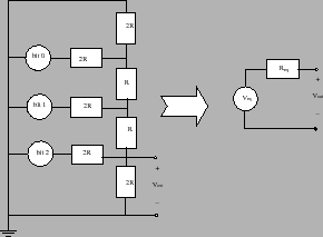
Op-amps have a variety of uses. One use is as a so-called buffer. A buffer is something that isolates or separates one circuit from another. In order to explain this more precisely, let's take a closer look at our 3-bit DAC.
The 3-bit DAC constructed in the previous lab produced a
digitally controlled voltage, but it turns out that we
can't really use this voltage as a source to drive
other circuits. The problem is that if we were to attach
another circuit to our DAC, then we would be changing the
![]() ladder network and hence would change the voltage
produced by that network. We refer to this phenomenon as
loading. The problem with our circuit is that it
produces a voltage that is not insensitive to the
load on the circuit.
ladder network and hence would change the voltage
produced by that network. We refer to this phenomenon as
loading. The problem with our circuit is that it
produces a voltage that is not insensitive to the
load on the circuit.
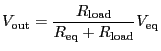
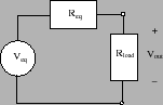
We now use our preceding discussion about Thevenin circuits to study the loading problem. Our preceding discussion asserted that a simpler circuit known as the Thevenin equivalent can always produce the output voltage of any resistive network with independent sources. Figure 4 shows the original DAC network (assuming only one of the output pins is high) and its associated Thevenin equivalent.
Assuming that the Thevenin equivalent voltage ![]() and resistance
and resistance ![]() are known, then we can go ahead
an determine the effect that a load resistance has on the
circuit's output voltage by a simple application of the
voltage divider law. If we place a load with resistance
are known, then we can go ahead
an determine the effect that a load resistance has on the
circuit's output voltage by a simple application of the
voltage divider law. If we place a load with resistance
![]() between the DAC's output node and ground,
then the loaded Thevenin equivalent circuit would be as
shown in figure 5 and the resulting output
voltage would be
between the DAC's output node and ground,
then the loaded Thevenin equivalent circuit would be as
shown in figure 5 and the resulting output
voltage would be
Remember that ![]() is the open circuit voltage
generated by the circuit and this is precisely the voltage
that we wanted our DAC to generate. Since the resistances
is the open circuit voltage
generated by the circuit and this is precisely the voltage
that we wanted our DAC to generate. Since the resistances
![]() and
and ![]() are positive, this means
that the ratio.
are positive, this means
that the ratio.
![]() must be less than one. In other words, the output voltage
of the loaded DAC will always be less than what we want it
to be.
must be less than one. In other words, the output voltage
of the loaded DAC will always be less than what we want it
to be.
As a numerical example, let's assume that ![]() is 1
k-ohm and let's assume that
is 1
k-ohm and let's assume that ![]() equals 8 ohms.
This rather low load resistance is common for some devices
such as audio speakers. The ratio is now readily seen to
be
equals 8 ohms.
This rather low load resistance is common for some devices
such as audio speakers. The ratio is now readily seen to
be
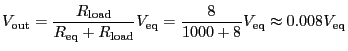 |
The bottom line in our preceding discussion is that
connecting a load to a circuit always effects the output
voltage that the circuit will generate. We can minimize
the sensitivity of the output voltage to the load
resistance by designing the circuit so its Thevenin
equivalent resistance, ![]() , is large. From
equation 1, we see that the ratio
, is large. From
equation 1, we see that the ratio
![]() can be made arbitrarily
small by selecting
can be made arbitrarily
small by selecting ![]() arbitrarily large.
arbitrarily large.
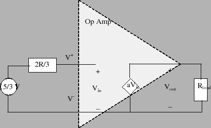
In order for our DAC to be useful, we'll need to find a way of redesigning the DAC, so that its Thevenin equivalent output resistance is very large. If this is done, then the output voltage generated by the DAC will be insensitive to variations in the load resistance. We can accomplish this feat by simply augmenting our existing ladder network with a buffering amplifier.
A buffer is a unity-gain amplifier that has an extremely
high input resistance and an extremely low output
resistance. This means that the buffer can be modelled as
a voltage controlled voltage source that has a gain of
one. We connect the buffer to our DAC as shown in figure
6. Note that we've represented the DAC by
its Thevenin equivalent circuit. Since the buffer has an
infinite input resistance, there is no loading effect so
that
![]() . Moreover, we know that
the output voltage produced by the buffer must be equal to
. Moreover, we know that
the output voltage produced by the buffer must be equal to
![]() since it has a gain of 1. In other words the
voltage produced by the buffer is precisely the voltage
generated by the DAC. The output voltage from the buffer
is insensitive to the load resistance because the
idealized buffer has an output resistance that is
essentially zero. By placing a unity gain buffer between
the DAC and the load, we have, therefore, solved our
loading problem.
since it has a gain of 1. In other words the
voltage produced by the buffer is precisely the voltage
generated by the DAC. The output voltage from the buffer
is insensitive to the load resistance because the
idealized buffer has an output resistance that is
essentially zero. By placing a unity gain buffer between
the DAC and the load, we have, therefore, solved our
loading problem.
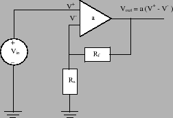
Unity gain buffers are idealized circuit elements. While it is possible to buy integrated circuits that serve as these idealized buffers, it is easy to build your own buffer from an operational amplifier. Recall that the op-amp has a large gain, near infinite input resistance and near zero output resistance. In order to turn it into a unity gain buffer, all we need to do is find a way of reducing the overall gain of the op-amp to unity. This can be done using the non-inverting op-amp circuit shown in figure 7. You will be asked to analyze this circuit as part of the pre-lab.