|
|
|
Dept. of Electrical Engineering
University of Notre Dame
261 Fitzpatrick Hall
Notre Dame, IN 46556
(574) 631-5693
fax: (574) 631-4393
pfay@nd.edu |
|
|
|
|
Education
Ph.D., Electrical Engineering July 1996
University of Illinois at Urbana-Champaign GPA: 5.0/5.0
Thesis Advisor: I. Adesida
Thesis Title: A High Speed Monolithically Integrated Photoreceiver for Long Wavelength Communication Systems
M.S., Electrical Engineering May 1993
University of Illinois at Urbana-Champaign GPA: 5.0/5.0
Thesis Advisor: J. Lyding
Thesis Title: Scanning Tunneling Microscope Based Lithography on Silicon (100) for Microelectronic Device Fabrication
B.S., Electrical Engineering May 1991
University of Notre Dame GPA: 3.96/4.0
Research and Teaching Experience
Professor, August 2008 to present
Associate Professor, August 2003 to 2008
Assistant Professor, August 1997 to 2003
University of Notre Dame
- Director of Notre Dame Nanofabrication Facility (NDNF), January 2003 to present
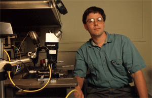
- Established High Speed Circuits and Devices Laboratory featuring analog electronic device and circuit characterization at frequencies up to 1 THz (including vector network analysis to 750 GHz, spectrum analysis, modulation analysis, noise figure measurement, mixer characterization, detection spectral response), digital circuit testing to 40 Gb/s, optoelectronic device characterization to 50 GHz, variable-temperature device and circuit characterization, and device-level characterization including current-voltage and capacitance-voltage measurement, optical photoresponse characterization at wavelengths from 200 nm to 12 µm, deep-level transient spectroscopy, and low-frequency noise spectroscopy
- Established externally-funded research program in high-speed electronic and optoelectronic devices and circuits. Research emphasis on compound semiconductor microelectronics (including design and fabrication of HEMTs, HFETs, MISFETs, HBTs, RTDs, heterostructure photodetectors, and millimeter-wave detectors), circuit demonstrations of device technologies, development and use of micromachining techniques for the fabrication of microwave components, sensors, and packaging
- Developed and taught graduate-level course in optoelectronic devices and applications
- Developed advanced undergraduate/graduate level microwave circuit design and microwave measurements course and associated instructional Microwave Circuit Design and Measurements Laboratory (EE 40458, 60558)
- Revised and taught Electronics II course and laboratory (EE 30342) 2003-07, 2014-16
- Participated in the development of a new multidisciplinary first-year engineering course sequence (EG 111/112); taught EG 112 during 2001-2002
- Revised and taught Electronics I course and lab (EE 20242) 1998-2000, 2008-2010
Visiting Assistant Professor, August 1996 to August 1997
Visiting Postdoctoral Research Associate, August 1996 to August 1997
University of Illinois at Urbana-Champaign
- Responsible for teaching undergraduate solid-state physics and devices course and integrated circuit technology course
- Investigated advantages and achievable performance of several approaches to monolithic integration for optoelectronic integrated circuit (OEIC) fabrication. OEICs for long-wavelength photoreceiver applications using p-i-n and MSM photodetectors and high electron mobility transistors (HEMTs) designed, fabricated, and characterized.
Research Assistant, August 1991 to July 1996
University of Illinois at Urbana-Champaign
- Designed, fabricated, and tested high-speed (>18 GHz) monolithic optical MSM/HEMT receivers for 1.55 µm wavelength fiber optics communication. Microwave circuit design completed using Hewlett-Packard's MDS circuit simulation package; RF characterization of discrete devices and complete system using both frequency- and time-domain methods
- Developed several lithographic processes for high-resolution electron-beam lithography suitable for fabrication of optoelectronic integrated circuits and monolithic microwave integrated circuits with Cambridge EBMF 10.5
- Characterized surface damage due to reactive-ion etching processing in InAlAs/InGaAs/InP heterostructure FETs and its impact on FET performance
- Developed silicon nitride-based passivation process for InAlAs/InGaAs heterostructure FETs, and characterized the effect of the process on device performance
- Developed and characterized several wet etches useful in the fabrication of integrated circuits in the InAlAs/InGaAs/InP material system
- Refined STM-induced oxidation of silicon (100) surface, and used it to modify NMOS device behavior
Scholarships and Fellowships
- Tau Beta Pi Graduate Research Fellow (1991-1992)
- National Science Foundation Graduate Research Fellow (1992-1995)
- University of Illinois Graduate College Fellow (1991-1992)
Honors and Awards
- Fellow of IEEE; citation: for contributions to compound semiconductor tunneling and high-speed device technologies, 2016
- College of Engineering Outstanding Teacher Award, 2015
- IEEE Electron Device Society Distinguished Lecturer, 2015
- Co-recipient of Best Student Poster award, Broadband Wireless Access & Applications Center conference, May 2014
- Co-recipient of IEEE Transactions on Advanced Packaging Best Paper Award, 2007
- Senior Member of IEEE, March 2002
- IEEE Outstanding Teacher Award, Dept. of Electrical Engineering, 1998-1999
- Finalist, Society for the Advancement of Materials and Process Engineering's award program, 1991
- U.S. Patent #5,880,482 awarded for "Low Dark Current Photodetector," March 9, 1999
- U. S. Patents #7,608,919 and 7,612,443 for “System for Inter-Chip Communication,” October 27, 2009 and November 3, 2009, respectively.
- U.S. Patent #8,021,965 awarded for “Inter-Chip Communication,” September 20, 2011.
- U.S. Patent #8,592,859 awarded for “Methods and Apparatus for Antimonide-Based Backward Diode Millimeter-Wave Detectors,” November 26, 2013.
- U.S. Patent #8,623,700 for “Inter-Chip Communication,” awarded January 7, 2014.
- U.S. Patent #8,796,733 awarded for “Low Voltage Tunnel Field-Effect Transistor (TFET) and Method of Making Same,” August 5, 2014.
Professional Memberships
- Member of Eta Kappa Nu, Tau Beta Pi
- Fellow of IEEE
- Member of IEEE Electron Device Society, Microwave Theory and Techniques Society, IEEE Photonics Society, IEEE Components, Packaging, and Manufacturing Technology Society
