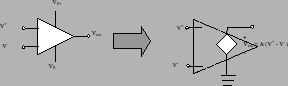
The idealized model shown in figure 8 is a good approximation for the ``real-life'' op-amp's behavior. In other words, the op-amp is a special circuit that has been specially engineered to behave like its idealized circuit model. We can therefore use op-amp models in a reliable manner to predict the behavior of op-amp circuits, with high confidence that our analytical predictions will hold true in real-life. This means the op-amp is a useful building block in analog circuit design.
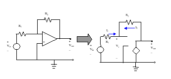
The fact that the operational amplifier has an extremely large voltage gain is very useful when we connect the op-amp in a feedback circuit. In particular let's consider the inverting feedback connection shown in figure 9. This circuit shows the positive terminal of an independent source connected to the inverting terminal of the op-amp through a resistor ![]() . A portion of the output voltage,
. A portion of the output voltage, ![]() is applied to the inverting input terminal through the voltage divider formed by resistors
is applied to the inverting input terminal through the voltage divider formed by resistors ![]() and
and ![]() . In other words, a portion of
. In other words, a portion of ![]() is fed back into the op-amp's input, hence the name ``feedback circuit''.
is fed back into the op-amp's input, hence the name ``feedback circuit''.
To analyze this circuit, we want to derive the relationship between the input voltage ![]() and the output voltage
and the output voltage ![]() . In particular, we note that
. In particular, we note that
Under the virtual ground assumption, we know that the current ![]() through resistor
through resistor ![]() must be
must be
![]() . We also know that the current,
. We also know that the current, ![]() , through the feedback resistor,
, through the feedback resistor, ![]() , must be
, must be
![]() . Moreover, we know that the input resistance of the op-amp is extremely large so that
the current going into the negative terminal is also nearly zero. By Kirchoff's law, we can therefore conclude that
. Moreover, we know that the input resistance of the op-amp is extremely large so that
the current going into the negative terminal is also nearly zero. By Kirchoff's law, we can therefore conclude that ![]() . Because the current going through both resistors is nearly the same, we can immediately see that
. Because the current going through both resistors is nearly the same, we can immediately see that
Note that the above analysis is approximate in the sense that we used the high gain of the op-amp to assume that the negative terminal was at ground (the virtual-ground assumption) and we used the high-input resistance of the op-amp to show that the current through ![]() and
and ![]() were equal to each other. It is because of these approximations that we find that the voltage gain of the inverting feedback connection is insensitive of the op-amp's gain.
were equal to each other. It is because of these approximations that we find that the voltage gain of the inverting feedback connection is insensitive of the op-amp's gain.
Finally note that the preceding analysis can also be used with slight modifications to derive the voltage gain for the non-inverting op-amp feedback circuit shown in figure 7. As part of the pre-lab, you will need to do this analysis.