The MicroStamp11's SPI interface uses four pins. These are
pins 15-18. They correspond to bits PD2 through PD5 on
PORTD. The clock line comes out of pin PD4 with the
logical name SCK. This line is a 50 percent duty
cycle clock whose rate can be controlled by the programmer.
There are two data lines. The master-out slave-in
(MOSI) line is on pin PD3. It is used to clock data out to
the slave device from the MicroStamp11. The master-in
slave-out (MISO) line is on pin PD2. This pin is used to
clock data into the MicroStamp11 from the slave device. In
addition to the clock and data lines, there is an
additional control line with the logical name SS
(slave select) This control line is on pin PD5. The
slave-select (SS) pin is an optional control line that can
be used when the channel is active. It is often used to
signal the end or beginning of a transmission.
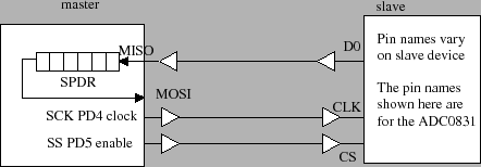
Figure 5 shows how the SPI interface is
constructed. The data (MOSI/MISO) pins are connected to an
8-bit data register with logical name SPDR. When a
data transfer operation is performed, this 8 bit register
is serially shifted eight positions and the data is
transmitted to or received from the slave. Figure
5 illustrates the pins and their
connection to the SPDR buffer assuming that a serial
IC (ADC0831) is clocking data into the MicroStamp11 over
the MISO pin.
Using the SPI subsystem to output data to the shift
register is relatively easy with the kernel function
provided in the lab. The kernel function is
shiftout(). This function clocks out an 8 bit
frame at a specified rate over the MOSI line. This
function is blocking, which means that the
function will not return until the data has actually been
transmitted by the MicroStamp11. We've also included a
function shiftin that can be used to clock data
into the MicroStamp11 from the slave device. A more
detailed description of both kernel functions is provided
below:
void shiftout(unsigned char data, unsigned char rate)
Description: This function clocks out a byte of data
stored in data at the rate specified by
rate. The function first sets PD3-5 to output and
then sets these lines low. The data is then clocked out
over pin PD3 using pin PD4 as the clock. After the data
has been clocked out the function toggles line pin PD5
(slave-select) to signal to the slave that it is finished.
Usage: The following code segment
 digitdata = 0x3F;
 shiftout(digitdata,SPI_62kHz);
transmits the binary number
unsigned char shiftin(unsigned char rate)
Description: This function clock in a byte of data
and returns the data as an unsigned character. The data
is clocked in at a rate specified in the function's rate
argument. Prior to clocking in the data, the function
toggles the slave select line (PD5) to inform the slave
that it is ready to receive data.
Usage: ddata=shiftin(SPI_62kHz);
rate
argument are defined in the following table.
| logical name | transfer frequency |
SPI_1MHz |
1 MHz |
SPI_500kHz |
500 kHz |
SPI_125kHz |
125 kHz |
SPI_62kHz |
62.5 kHz |