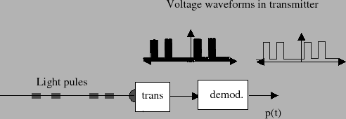
The purpose of the receiver is to translate the received IR pulses into a set of pulsed voltage levels representing information. We can think of the receiver as simply undoing what the transmitter has done as is shown in figure 7.
As can be seen in figure 7, our system
consists of two parts. The trans subsystem
translates the received IR energy into a voltage waveform.
Ideally the trans subsystem removes the IR frequency
from the received signal so we are left with the modulated
carrier signal ![]() that was originally generated by
the transmitter. In practice, the channel may have
introduced some distortion so that the received
that was originally generated by
the transmitter. In practice, the channel may have
introduced some distortion so that the received ![]() may not look exactly like the transmitter's
may not look exactly like the transmitter's ![]() . The
modulated carrier is then demodulated in the
. The
modulated carrier is then demodulated in the
demod subsystem. This subsystem removes the carrier
wave, so we are left with the original signal ![]() that
the transmitter started with.
that
the transmitter started with.
While the conceptual function of the trans and
demod subsystems is straightforward, the actual
implementation can be somewhat more involved. This is
because the receiver's performance must be robust to
distortions introduced by the channel. In practice,
therefore, the trans and demod subsystems
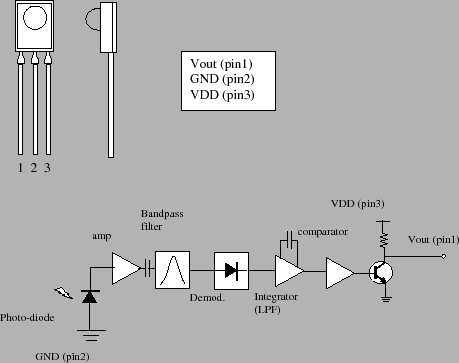
consist of additional subsystems. In figure
8 we show the block diagram for an
integrated circuit (IC) that incorporates the
photodetection, transducer, and demodulation functions into
a single chip. Let's step through this block diagram.
The IR beam is received by a photodiode shown on the left hand side of figure 8. The output of the photo-diode goes through a buffering amplifier which is then fed through a bandpass filter. The purpose of the bandpass filter is to only select out those frequencies in the neighborhood of the carrier wave. So if there are additional frequency components in the received signal (due perhaps to the channel), these are removed by the bandpass filter. The output of the bandpass filter goes through a demodulator. The demodulator consists essentially of a diode whose purpose is to rectify the signal. The rectified signal is sent through a lowpass filter to remove high frequency harmonics that may have been introduced by the rectification function. The final signal leaving the lowpass filter will not be a sharp set of pulses (due to distortion introduced by the channel and our demodulator's filter functions), so we introduce a comparator to "clean-up" the distorted pulses received by the module. The output of the modulator then feeds a single transistor current source.
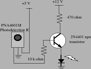
The use of the PNA4601 receiver module makes the design of your IR link receiver very easy. Essentially, all you need to do is connect up the module to a current source and an LED. The basic circuit schematic for the receiver circuit (not including the LED) is shown below in figure 9.