The purpose of the transmitter is to transform the
information we want to send into a signal that can be
propagated by the channel. In the case of our wired copper
channel, this means we want the information to be
transformed into a modulated voltage level, something like
the pulse train in figure 1. For a wireless
channel, however, the transmitter needs to encode the
information onto an EM wave that can be easily propagated.
In this lab, this means that the transmitter needs to take
the voltage pulses generated by the ![]() Stamp11 and it
needs to put them onto an infra-red EM wave. We usually
refer to this encoding as modulation.
Stamp11 and it
needs to put them onto an infra-red EM wave. We usually
refer to this encoding as modulation.
Let ![]() be a time-varying signal representing the bits
of information we want to transmit over the channel. A
possible waveform for
be a time-varying signal representing the bits
of information we want to transmit over the channel. A
possible waveform for ![]() is shown in figure
1. The transmitter then uses this signal to
modulate a sinusoidal (or square) wave with a frequency
is shown in figure
1. The transmitter then uses this signal to
modulate a sinusoidal (or square) wave with a frequency
![]() . We refer to this sinusoidal wave as the
signal's carrier wave. For the wireless channel
we're building, standard receiver structures usually assume
a carrier wave with a frequency between
. We refer to this sinusoidal wave as the
signal's carrier wave. For the wireless channel
we're building, standard receiver structures usually assume
a carrier wave with a frequency between ![]() kHz. The
carrier wave is added to assist in subsequent signal
processing at the receiver end. So the information that
the transmitter generates has the form
kHz. The
carrier wave is added to assist in subsequent signal
processing at the receiver end. So the information that
the transmitter generates has the form
The signal ![]() in equation 2 is still
an electrical signal that has been generated by the
transmitter. The transmitter must now use this signal to
amplitude modulate the IR beam we intend to transmit
through the channel. So the strength of the IR beam that
is actually transmitted by the system has the functional
form
in equation 2 is still
an electrical signal that has been generated by the
transmitter. The transmitter must now use this signal to
amplitude modulate the IR beam we intend to transmit
through the channel. So the strength of the IR beam that
is actually transmitted by the system has the functional
form
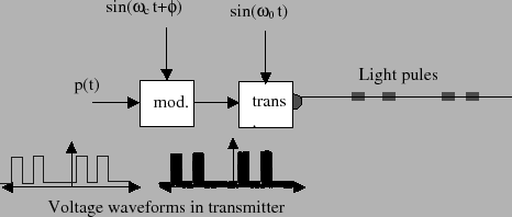
Figure 4 illustrates the steps
outlined above. The information signal ![]() is mixed
with the carrier wave in the block label
is mixed
with the carrier wave in the block label mod. At
the bottom of the figure, you'll see representative
waveforms for the voltages in the transmitter that enter
and exit the mod system block. The output of the
modulator is then used by the trans (transducer)
block in the system. The transducer block uses this
voltage waveform to modulate the IR wave. This IR beam is
then sent out into the channel (air) to be caught by the
receiver.
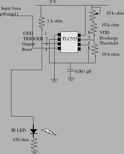
In this lab, you'll need to build a circuit that performs the basic modulation and transducer functions shown in figure 4. A schematic diagram for the entire transmitter circuit is shown in figure 5. The modulator function is carried out by the 555 timer IC shown in the top part of the schematic. The transducer function is performed by the photo-diode circuit shown on the bottom part of the figure.
The 555 timer IC (TLC555) is a standard IC chip that is
used to generate very precise clock pulses. It is also
possible to use the ![]() Stamp11 to generate the clock
pulses, but this puts a heavy burden on the
micro-controller. Using the TLC555 IC relieves the
micro-controller from this burden, thereby freeing it up to
do more useful things. The clock signals generated by the
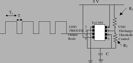
TLC555 are shown below in figure 6.
Stamp11 to generate the clock
pulses, but this puts a heavy burden on the
micro-controller. Using the TLC555 IC relieves the
micro-controller from this burden, thereby freeing it up to
do more useful things. The clock signals generated by the
TLC555 are shown below in figure 6.