We will later use the output of the comparator circuit as an input to the MicroStamp11. There is, however, a big problem with this approach. The problem is that the voltage levels generated by the comparator circuit are too large. Recall that for the op-amp to work well, the supply voltage must be around 9 volts. This means that the output voltage of your comparator will be either 0 or 9 volts. If we were to apply the 9 volt output to an input pin of the MicroStamp11 we would immediately destroy the MicroStamp11. The MicroStamp11 is only designed to accept voltages that are either zero or 5 volts. Any applied voltages outside of this range will destroy the delicate circuitry within the device. So if we are to use the output of the comparator, we will need some way of reducing the 0-9 volt range produced by the comparator to a 0-5 volt range. This can be done using a clamp circuit.
A clamp circuit is a special type of circuit that is
used to limit or clamp the output voltage to a
specified range. The clamping action is accomplished
through the use of diodes. Remember that a diode is like
an electronic valve. When it is forward biased, it acts
like a short circuit and when it is reverse biased it acts
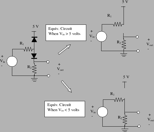
like an open circuit. Figure 10 depicts the
schematic for a clamp circuit. When ![]() is
greater than 5 volts, then the bottom diode is reverse
biased and the top diode is forward biased. As a result,
the circuit can be replaced by the equivalent circuit shown
in the top righthand drawing. In this case, we see that
the input source is connected directly to the 5 volt supply
and it is disconnected from the resistor
is
greater than 5 volts, then the bottom diode is reverse
biased and the top diode is forward biased. As a result,
the circuit can be replaced by the equivalent circuit shown
in the top righthand drawing. In this case, we see that
the input source is connected directly to the 5 volt supply
and it is disconnected from the resistor ![]() . This
means, therefore that
. This
means, therefore that ![]() will equal zero. The
resistor
will equal zero. The
resistor ![]() is put in here to limit the current drawn
out of voltage source
is put in here to limit the current drawn
out of voltage source ![]() . If
. If ![]() is
less than 5 volts, then the bottom diode is forward biased
and the top diode is reverse biased. The equivalent
resistive network is shown in the bottom righthand
schematic diagram. We now see that the source is connected
to ground through resistors
is
less than 5 volts, then the bottom diode is forward biased
and the top diode is reverse biased. The equivalent
resistive network is shown in the bottom righthand
schematic diagram. We now see that the source is connected
to ground through resistors ![]() and
and ![]() . Once again we
choose
. Once again we
choose ![]() to be larger than
to be larger than ![]() so that most of
so that most of
![]() drops over the second resistor.
drops over the second resistor.
The choice of ![]() and
and ![]() in the above circuit is
dictated by two concerns. First we see that
in the above circuit is
dictated by two concerns. First we see that ![]() is
essentially a current limiting resistor that prevent the
source from being unduly stressed if
is
essentially a current limiting resistor that prevent the
source from being unduly stressed if
![]() . A
logical value for this would be around 1 k-ohm.
. A
logical value for this would be around 1 k-ohm. ![]() is
then chosen to be much larger than
is
then chosen to be much larger than ![]() in order to drop
most of the input voltage across this second resistor.
Choosing
in order to drop
most of the input voltage across this second resistor.
Choosing ![]() an order of magnitude greater than
an order of magnitude greater than ![]() is
a realistic choice.
is
a realistic choice.