The output compare event is a hardware event tied to the
micro-controller's real-time clock. The real-time clock on
the ![]() Stamp11 is a hardware subsystem within the
Stamp11 is a hardware subsystem within the ![]() Stamp11
that provides a very precise and steady time reference. In
particular, the clock increments a hardware register whose logical
name is
Stamp11
that provides a very precise and steady time reference. In
particular, the clock increments a hardware register whose logical
name is TCNT. TCNT is a 16-bit unsigned counter. It
is incremented at a rate that is determined by two bits in a
control register TMSK2.
The rate at which TCNT is incremented is determined by the
bits PR1 (0x02) and PR0 (0x01)
in TMSK2. The following commands
  TMSK2 &= ~0x01;
  TMSK2 &= ~0x02;
clear the
PR0 and PR1 bits in TMSK2
and causes TCNT to be incremented once every 500
nanoseconds. Other update rates are shown in the
following table under the assumption that the
| PR1 | PR0 | TCNT clock rate |
| 0 | 0 | 407 nsec |
| 0 | 1 | 1.628 |
| 1 | 0 | 3.255 |
| 1 | 1 | 6.511 |
The counter TCNT cannot be reset or stopped by the
user. So to generate timing events, we compare the value
in TCNT against another number that is held in an
output compare register. When the value in
TCNT matches the number in the output compare
register, we trigger an output-compare event. The
Motorola 68HC11 micro-controller has 5 different output
compare registers so it is possible to trigger 5 different
output compare events . These registers have the logical
names TOC1, TOC2, TOC3, TOC4,
and TOC5. The exact addresses of these registers
will be found in the include file hc11.h.
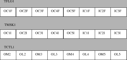
Figure 3 shows the three registers used by
the output compare interrupt. These three registers are
TMSK1, TFLG1, and TCTL1. The register
TMSK1 is a control register that is used to "arm"
the interrupt. The register TFLG1 is a status
register that can be used to "acknowledge" the servicing of
a caught interrupt. Register TCTL1 is used to
modify the way in which the output compare interrupt
interacts with the micro-controller's output pins.
Output compare events are generated in the micro-controller's hardware. This event will result in a hardware interrupt (also called an output compare interrupt) being generated if:
Arming an interrupt means to enable the source of the
interrupt. We arm an interrupt by setting the
appropriate bit in a hardware register. Output compare
interrupts are armed by setting bits in the register
TMSK1. The output compare 4 (OC4) interrupt, for
example, is enabled by setting bit OC4I in register
TMSK1 to 1 (see figure 3).
Enabling the interrupt means that the software pays
attention to the interrupt. We enable all interrupts
by clearing the I bit in the condition code register of the
micro-controller. This bit is usually cleared in the
init() function using the assembly command
cli.
Acknowledging an interrupt means that we tell the system
that a previously received interrupt has been serviced. We
acknowledge an interrupt by setting the appropriate
bit in the status register TFLG1. When an interrupt
is caught by the software, an appropriate bit in
TFLG1 is cleared (set to zero). This status
register allows us to explicitly determine the source of
the interrupt. If, however, we want our system to catch the
next interrupt, we must explicitly acknowledge that the
interrupt was caught and this acknowledgement is performed
by setting the appropriate bit in TFLG1 to one. So,
for example, we acknowledge the OC4 interrupt by
setting bit OC4F in TFLG1 to 1 (see figure
3).
When the interrupt is caught by the software, program execution jumps to the interrupt vector and begins executing the instructions at that location. The user can install a special interrupt service routine (ISR) at this interrupt vector through the use of special compiler directives. We'll discuss how you go about writing an ISR in the next section.
The output compare event can also be used to effect
specific output pins. The TCTL1 register determines
what effect the OC2, OC3, OC4, and OC5 events will have on
the output pin. The layout for the TCTL1 register is given
in figure 3. The logical names for the bits
in this register are ![]() and
and ![]() where
where ![]() takes values
between 2 and 5. The following table itemizes the effect
that the bits in
takes values
between 2 and 5. The following table itemizes the effect
that the bits in TCTL1 have on the output pins.
| OMx | OLx | Effect when TOCx=TCNT |
| 0 | 0 | Does not effect OCx |
| 0 | 1 | toggle OCx |
| 1 | 0 | clear OCx (set to zero) |
| 1 | 1 | set OCx (set to 1) |
The OC events OC2, OC3, and OC4 are tied to pins PA6, PA5, and PA4, respectively, on PORTA. Recall that these pins only have the direction state of "output". The other output-compare event, OC5, is tied to pin PA3 on PORTA. This is a bidirectional pin and this means that to use TCTL1 to effect PA3, we'll need to set its direction state to output. The OC1 event uses the output pin somewhat differently than OC2-OC5 and we won't discuss its use in this course. Output-compare events OC2-OC5, however, have easily defined functions. Namely that when the event OCx occurs, the state of the output pin PAx changes from 0 to 1 or vice versa, depending upon how the bits OMx and OLx are set. This can be extremely useful if we are attempting to have the micro-controller generate output voltages quickly in response to output compare events. Because the pin state changes are handled in hardware, this effect can be manifested very quickly. If we were to attempt to do the same thing in software, it could potentially take a long time for the ISR to execute and this can dramatically destabilize a program's real-time behavior.