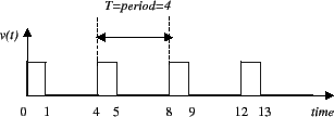
In this section, we discuss the RC circuit's (figure
2) response to an input signal that is a
pulse width modulated signal of known period and duty
cycle. The pulse width modulated input signal is shown in
figure 6. Over a single period, ![]() , the
input voltage to the circuit has two distinct parts. There
is the "charging" part from
, the
input voltage to the circuit has two distinct parts. There
is the "charging" part from ![]() during which the
applied voltage is
during which the
applied voltage is ![]() . In this interval, the capacitor is
being charged by the external voltage source. The second
part is the "discharging" part from
. In this interval, the capacitor is
being charged by the external voltage source. The second
part is the "discharging" part from ![]() . During this
interval the applied voltage is zero and so the capacitor
is discharging through its resistor.
. During this
interval the applied voltage is zero and so the capacitor
is discharging through its resistor.
During the "charging" phase, we can think of the RC
circuit as being driven by a step function of magnitude
![]() volts. If we assume that the capacitor has an initial
voltage of
volts. If we assume that the capacitor has an initial
voltage of ![]() at the beginning of the charging phase
(time
at the beginning of the charging phase
(time ![]() ), then the circuit's response is simply given
by equation 2 for
), then the circuit's response is simply given
by equation 2 for ![]() .
.
During the "discharge" phase, there is no external voltage
being applied to the RC circuit. This means that the
system response is due solely to the capacitor voltage
that was present at time ![]() after the charging period.
As a result, the capacitor's voltage over the time
interval
after the charging period.
As a result, the capacitor's voltage over the time
interval ![]() is simply the RC circuit's natural
response. This means, of course, that the capacitor
voltage for
is simply the RC circuit's natural
response. This means, of course, that the capacitor
voltage for ![]() is given by equation
1 of the form
is given by equation
1 of the form
![]() for
for ![]() ,
where the initial voltage,
,
where the initial voltage, ![]() , is the voltage on the
capacitor at time
, is the voltage on the
capacitor at time ![]() .
.
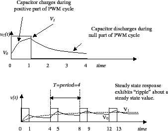
The top drawing in figure 7
illustrates the output signal we expect from a PWM signal
driving an RC circuit over an interval from ![]() . For
times beyond this interval, we
expect to see the waveform shown in the bottom drawing in
figure 7. In this drawing we
assume that the capacitor is initially uncharged. As our
circuit cycles through its charge and discharge phases, the
voltage over the capacitor follows a saw-tooth trajectory
that eventually reaches a steady state regime. In this
steady-state region, the capacitor on the voltage zigzags
between
. For
times beyond this interval, we
expect to see the waveform shown in the bottom drawing in
figure 7. In this drawing we
assume that the capacitor is initially uncharged. As our
circuit cycles through its charge and discharge phases, the
voltage over the capacitor follows a saw-tooth trajectory
that eventually reaches a steady state regime. In this
steady-state region, the capacitor on the voltage zigzags
between ![]() and
and ![]() volts. The exact value of these
steady state voltages is dependent on the period
volts. The exact value of these
steady state voltages is dependent on the period ![]() and
the duty cycle
and
the duty cycle ![]() .
.
The steady state region shown in figure
7 is usually characterized by
two "figures of merit". The first "figure of merit" is the mean voltage, ![]() ,
of
the steady state response and it is given by the equation
,
of
the steady state response and it is given by the equation
In this lab you will be using the output of the RC network
as the analog voltage generated by a digital-to-analog
converter (DAC). As you can see in figure
7, this analog voltage is not
really constant, it has a mean value and a small ripple.
So the performance of the RC-DAC can be characterized by
these two figures of merit. If our DAC performs well,
then its mean voltage ![]() must vary in a linear
manner with the commanded voltage and its ripple,
must vary in a linear
manner with the commanded voltage and its ripple, ![]() ,
should be very very small. In return for accepting a
small ripple, we gain some important benefits. In the
first place the DAC only needs to use a single output line
and the precision of the DAC increases significantly (from
3 to 6 bits).
,
should be very very small. In return for accepting a
small ripple, we gain some important benefits. In the
first place the DAC only needs to use a single output line
and the precision of the DAC increases significantly (from
3 to 6 bits).
The reason for the "increased" precision is that we are no longer using the output lines to encode the digital number we want to convert. Instead, we are using a time-varying signal (the PWM signal) to encode the voltage we wish to convert. We don't get something for nothing. In return for this enhanced DAC, we must settle for a small ripple on the converted voltage and our DAC's response time to changes in the requested voltage will be governed by our circuit's RC time constant.