![]()
![]()
![]()
![]()
![]()
![]()
Devices and circuit technologies for millimeter-wave detection and imaging are being researched. This technology has applications in security screening, avionics, and medical imaging among others.
| The technical approach being pursued is the use of InAs/AlSb/GaSb and Si/SiGe heterostructure backward diodes for detection, and monolithic integration of other electronic and passive components with these devices for compact imaging system applications. | 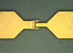 |
|||||
 |
||||||
|
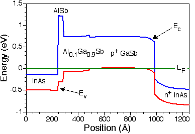
These devices are based on asymmetric tunneling induced by the broken-gap alignment possible in heterostructures between InAs and GaSb, or interband tunneling in p+/n+ Si/SiGe heterostructures. |
||||||
|
Comprehensive characterization of the devices, including DC characteristics, millimeter-wave sensitivity, nonlinear characterization, and noise measurements are key elements of this research effort. |
||||||
Recent demonstrations (selected):