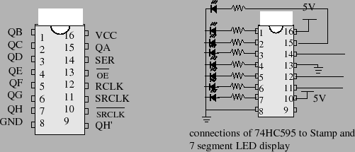
A serial-to-parallel device accepts a series of timed pulses and latches them onto a parallel array of output pins as shown in figure 1. This lab uses a rather simple integrated circuit (IC) known as an 8-bit serial-in/parallel-out shift register (74HC595) as the serial-to-parallel device. Figure 6 shows the pin out for the IC and shows how to connect the chip to the MicroStamp11 and the LED display.
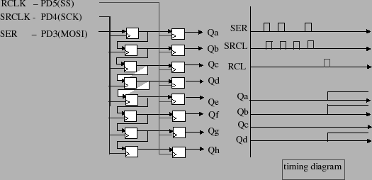
The basic idea is to send a sequence of bits (i.e., positive pulses) down to the serial-to-parallel chip (74HC595). The 74HC595 will then convert this serial input into a parallel input and latch the output so it continues to drive the LED display until the next series of bits is received and latched. This operation, however, requires some degree of control. For instance, we need some way of telling the chip when the pulses are expected to occur and we need some way of telling the chip when to latch the data. This means that we need two control lines to the chip, in addition to the data line.
To understand how these control lines work, we need to take a closer look at how the 74HC595 functions. The 74HC595 consists of an interconnected set of simpler digital circuits known as latches. There are actually two banks (columns) of latches, each column consisting of 8 latches. Figure 7 shows these two columns. The first column of latches form something known as a shift register. This bank accepts the serial input and shifts each bit in the series of input pulses down into the column. The second column of latches is used to store what is in the first column. This second column is connected to the chip's output and is used to drive the LED display. This frees up the first column to receive another series of inputs, without disrupting the actual signals delivered to the 7-segment display.
Each latch is a digital circuit with two inputs and one
output. The top input with the black arrowhead represents
the data and the other input with the white arrowhead
represents a control. The lines with the black arrowhead
are connected to the pin marked SER (serial input) and the
lines with white arrowheads are connected to the pin marked
SRCLK. This line is sometimes called the clock line. When
the data line (SER) is high and the control (SRCLK) is
high, then the output of the latch is also high until it is
reset. When the data (SER) is high and the control (SRCLK)
is low, then the output does not change from its previously
latched value. The first column of latches are daisy
chained together so the output of the top latch is the data
input to the second latch. What we do, therefore, is input
a bit string into SER along with a SRCLK signal. Each time
SRCLK goes high, the data in a latch is shifted to the
latch below it. We can therefore enter a string of 8 bits
into the first column of latches by sending each bit along
the SER line and then setting the SRCLK line high for each
bit of data. The timing diagram shown in figure
7 shows how the bit string 1011 is shifted
into the device. After the data has been shifted into the
first column, we transfer this data in parallel to the
second column of latches by setting the RCLK line
high.
This
second column of latches will retain their value until we
overwrite them with another RCLK signal.
In your design, you will need to connect the Microstamp11's data pin (MOSI) to the serial line ping (SER) on the latch. The clock signal is produced by the Microstamp on pin SCK. You need to connect SCK to pin SRCLK (source clock) in order to clock the data into the latch. Finally, you will need to use a control signal generated by the state select pin (SS) on the microstamp to latch the 74HC595's output. This means you will need to connect pin SS on the microstamp to pin RCLK on the latch.
Note that the kernel function shiftout() has been
written to coordinate the clock signal on SRCLK with
the latch signal generated by the slave select line
(SS) connected to the shift register's RCLK
pin. You might find it interesting to examine the source
code of the shiftout function and see if you can
explain how it works.