Facilities
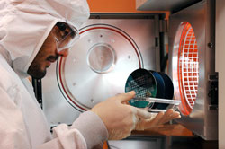 The NDNF is a CMOS and III-V semiconductor fabrication facility, comprising 9,000 sf, about half of which is class 100. Capabilities include pattern generation for mask making, contact and i-line projection optical lithography, 100 kV electron-beam direct write lithography, mask making, reactive-ion etching (RIE), inductively-coupled RIE (ICP-RIE, DRIE), plasma etching, thermal and electron-beam evaporation, dc and rf magnetron sputtering for metal and dielectric co-deposition, plasma-enhanced chemical vapor deposition (PECVD), atomic layer deposition, atmospheric-pressure CVD, low-pressure CVD, chemical-mechanical polishing (CMP), rapid thermal annealing and constant-temperature furnace thermal processing, and general wet chemistry, flip-chip die bonding, wire bonding, ribbon bonding, and die attach.
