“Quilted” Circuits
The semiconductor industry road map, which corresponds with Moore’s
Law and states that the density of chips doubles approximately every
18 months, is facing a bit of a roadblock. The experts agree: If
all else remains the same, the gains in cost and performance of monolithically
integrated chips are going to diminish substantially in the near
future, which means that the processing speed of computers will also
suffer.
A seamless
interface, tailor-made by Notre Dame faculty, may be just the thing to solve
the interchip interconnect problem. In fact, a research team led Gary
H. Bernstein, professor of electrical engineering, has demonstrated a new paradigm for interchip
communication called Quilt Packaging (QP).
 QP involves
the fabrication of contact nodules that protrude from the edge of a chip. The
chips needed to form a system are placed side-by-side, with the nodules allowing
a direct electrical interconnection. Linking together like the blocks of a card-trick
pattern quilt, the various integrated circuits can, in fact, be of heterogeneous
materials. In this way, for example, silicon processors could be combined efficiently
and inexpensively with optical processors, microwave devices, or memory. QP involves
the fabrication of contact nodules that protrude from the edge of a chip. The
chips needed to form a system are placed side-by-side, with the nodules allowing
a direct electrical interconnection. Linking together like the blocks of a card-trick
pattern quilt, the various integrated circuits can, in fact, be of heterogeneous
materials. In this way, for example, silicon processors could be combined efficiently
and inexpensively with optical processors, microwave devices, or memory.
This
type of interchip contact offers high-speed signal paths for the high-fidelity
transmission of signals between chips at very high frequencies, into the hundreds
of GHz. Signals could also be transferred between chips far more faithfully than
the conventional approach of going from one chip to another through packages
and printed circuit boards. The net result, as demonstrated by the team — Bernstein,
Patrick J. Fay, associate professor of electrical engineering; Gregory
L. Snider, professor of electrical engineering; and Qing
Liu, a graduate student in electrical
engineering — is a more efficient use of the die area and better performance
in an overall smaller system with the need for fewer chip packages. In short,
a better system is achieved at a lower cost.
The
team presented experimental results at the Second International Work-shop
on SOP, SIP, SOC (3S) Electronics Technologies in September 2006, where
they unveiled world-record transmission efficiencies at frequencies
up to 40GHz. “We used the equipment in the Notre Dame Nanofabrication
Facility to build and test the system,” says Bernstein, “and
we are very excited because this milestone shows that by using Quilt
Packaging, the cost of integrated systems, energy use, size, and weight
decreases, and performance can be improved. Additional studies may
impact portable devices such as laptops and cell phones but could also
improve the performance of high-speed systems, such as radar and microwave
communication systems.”
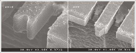
Self-aligning keys and slots bridge the gap between neighboring
chips, enabling direct chip-to-chip contact. The multi-chip “quilted” system
these links create offers high signal bandwidth, reduced power dissipation,
reduced production costs, and the option to use heterogeneous materials.
Nodules as small as 10 microns have been demonstrated by the Notre
Dame team in this National Science Foundation funded project. |