Facilities
Deposition Equipment

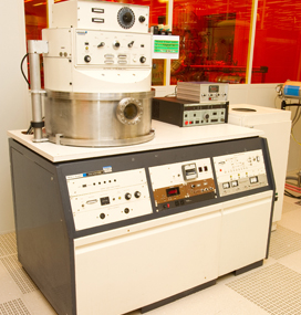
- Perkin-Elmer 2400 Sputtering System
- Manufacturer:
Randex - Operating Instructions
Description
The Randex Model 2400-8SA sputtering system is designed to deposit a wide variety of materials onto substrates such as ceramics, metals, plastics, glass, and semiconductors. The resulting thin films can range in thickness from a few Angstroms up to a fraction of a millimeter. This sputtering system can deposit in sequence up to three different materials onto a single substrate, thereby creating a sandwich-structured film such as multilayer optical interference filters. The system can also be used for ion etching, a process in which material is removed from, rather than deposited on, the substrate.
The Sputtering Process
Sputtering is a momentum transfer process in which atoms from a
cathode/target are driven off or sputtered by bombarding ions.
In this process, the momentum of bombarding ions is more important
than their energy. For example, a hydrogen or helium ion accelerated
to 3,000 eV will cause very little sputtering compared to an
ion of argon (which is chemically inert) with the same 3,000
eV energy, simply because the lighter hydrogen or helium ion
has much less momentum. Sputtered atoms travel until they strike
a substrate, where they deposit to form the desired layer. As
individual atoms they are chemically active and readily form
compounds with the ions and atoms of the bombarding gas. For
this reason inert argon is used as the bombarding gas. In some
applications however, a reactive gas is purposely added to argon
so that the deposited film is a chemical compound, and not the
elemental target materials. When argon ions strike the target
their electrical charge is neutralized and they return to the
process as atoms. If the target is an insulator, the neutralization
process results in a positive charge on the target surface. This
charge may reach the level where bombarding ions are repelled
and the sputtering process stops. To continue the process the
polarity must be reversed to attract enough electrons from the
discharge to eliminate surface charge. This periodic reversal
of polarity is done automatically by applying RF voltage onto
the target assembly (hence the term RF sputtering). Of interest
here is the diode rectifier-like behavior of the target and discharge
system. This is caused by the vast difference in mobilities of
ions and electrons; the electrons, which are much lighter, are
attracted in much greater numbers to the target during their
positive half-period of RF voltage than are the heavy ions during
their half-period.
Film types available: Cu, Ti, Ta, W, SiO2, AlSi, Cr, and 7059 glass.
Contact Information:
For additional information, please contact the NDNF staff at pfay@nd.edu.
2.10.15


