

|
 |
Student News |
| CSE Students Finish Ninth in ACM Contest <more> |
Dai Receives Honorable Mention at Bioengineering Conference <more> |
| Electrical Engineering Students Establish
Amateur Radio Club <more> |
| Engineering Industry Day Features 70 Companies <more> |
| Introduction to Engineering Program Hosts High School Students <more> |
| SWE Awards Scholarships to Notre Dame
Engineers <more> |
Alumni News |
| Carlos A. Paz deAraujo (B.S., EE ’99;
M.S., EE ’79; and Ph.D., EE ’82); Larry Augustin (B.S.,
EE ’84); Gerald M. Belian (B.S., CE ’62); James G. Berges
(B.S., EE ); John F. Daegele (B.S., EE ’83); Allen Hemberger
(B.S., CSE ’01); Casey Korecki (B.S., ME ’03); David Kowalski
(B.S., ME ’80); Mary Ledet (B.S., EE ’04); Jerome L. Margraf
(B.S., ME ’67); Richard O. Martin (M.S., EE ’ 64); Don
McBride (B.S., EE ’66); Edward J. Nowacki (M.S., EE ’67);
Haresh P. Patel (B.S., EE ’83); Gang Quan (Ph.D., CSE ’02);
Niel Ransom (Ph.D., EE ’73); James Schmiedeler (B.S., ME ’96);
Robert Stackowiak (B.S., CE ’78); William Stanchina (B.S., EE ’71);
Jim Tyler (B.S., ME ’86); and Jinhui Xu (Ph.D., CSE ’00). |
| To visit College of Engineering Alumni News <click here> |
New Instrument Produces Nanostructures without Lithography
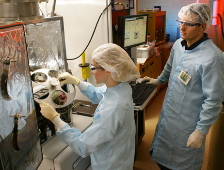
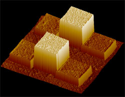
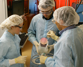
| A team of researchers led by Alan C. Seabaugh, professor of electrical engineering and associate director of the Center for Nano Science and Technology, has developed a new instrument capable of positioning vacuum-deposited metals, semiconductors, and dielectrics with nanometer-scale resolution without organic resists and customized masks (traditional lithography). Instead a precision nanopositioner is used to translate a substrate under a stencil mask between evaporation of dissilimar materials. This piezoflexure-enabled nanofabrication (PEN) techniquecan produced features at the nanometer scale. The PEN system allows for the clean characterization on surfaces near room temperature. |  |
 |
Copyright 2006. University of Notre Dame.