
Physical Characterization
Photovoltaic Characterization
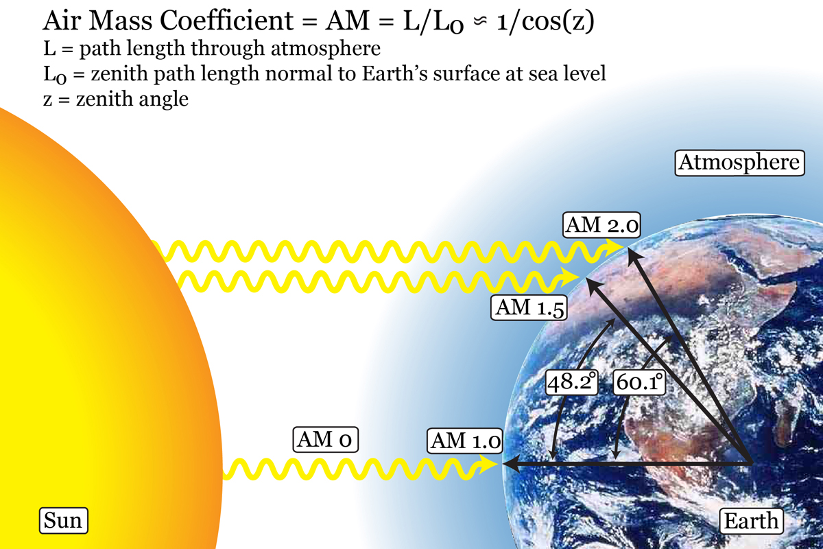
Figure. Schematic showing where AM 1.0, AM 1.5, and AM 2.0 irradiation is found on Earth as well as how the air mass coefficient is determined for other locations on Earth.
Photovoltaic cell performance is characterized using Air Mass 1.5 irradiation of 1000W/m2 (simulated solar light at the surface of the earth at 48.2°). Under illumination, we use a potentiostat to control the voltage between the two electrodes of the solar cell to measure the current/voltage characteristics of the device. Using the basic relationship Power = Current*Voltage, we are able to calculate the power output of the cell and, knowing the power of the incoming irradiation, the light to energy conversion efficiency.
By using a monochromater, a device that splits light into its individual colors much like a prisim, we can also monitor the incident photon to charge carrier efficiency, or IPCE. This metric allows us to see what fraction of incoming photons of a certain color are converted into electrons by our solar cell. This can tell us where our cell is the most efficient, and where it needs most work.
Using these, and other, methods, we are able to characterize the performance of our solar cells so that we can rationally design better, more efficient, cells.
Transmission Electron Microscopy (TEM)
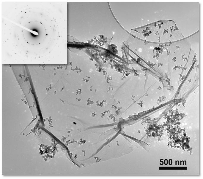
Figure. TEM image of graphene/TiO2 nanoparticle composite (left), and a graphene/TiO2/Ag composite (right).
The Titan 80-300 300 kV FEG Scanning Transmission Electron Microscope (TEM) in the Notre Dame Integrated Imaging Facility (NDIIF) is used to image samples on the smallest possible scales. By observing the deflection of very high energy electrons as they are transmitted through the sample, an image is constructed. The TEM system at Notre Dame can achieve angstrom resolution to image particles and surfaces on the atomic scale. The TEM is also equiped with a variety of other advanced diagnostic capabilites such as energy-dispersive X-ray spectroscopy (EDS or EDX), electron energy loss spectroscopy (EELS), electron diffraction, to further examine the atomic composition and structure of the sample. The Titan instrument is designed to perform in all TEM, STEM, EFTEM and EELS modes. It is capable of: • Fine structure imaging on atomic level • Angstroms resolution in S/TEM mode • Advanced energy resolution in EEELS for band gap and fine structures • Nano-scale resolution EDS in S/TEM mode • Maximum mechanical, electronic and thermal stability Features and specifications: • Energy spread - 0.7 eV • Point resolution - 0.2nm • Information limits - 0.1nm • STEM resolution - 0.135nm
Field Emission Scanning Electron Microscopy (FE SEM)

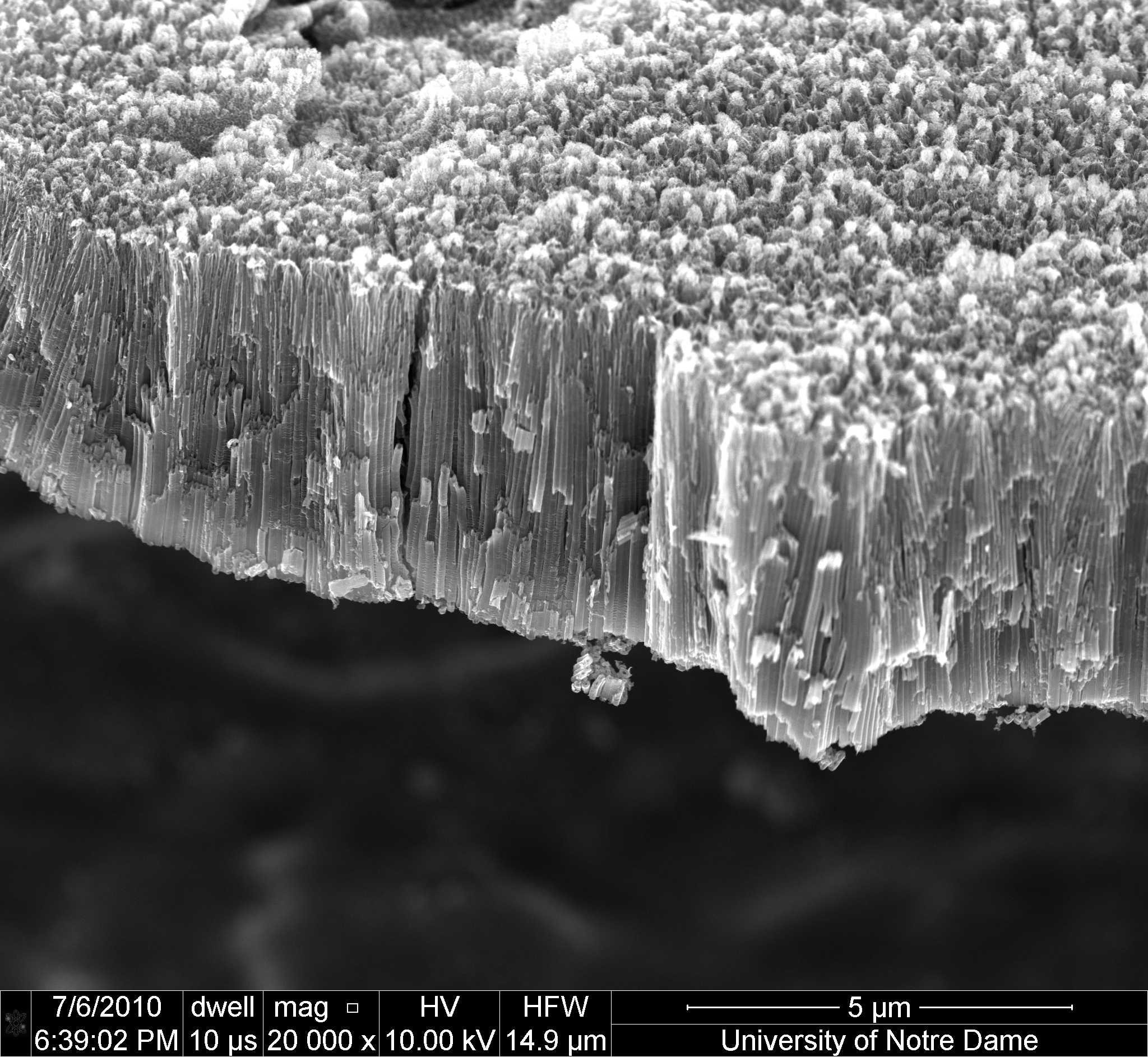
Figure. Cross sectional SEM image of TiO2 nanotubes grown by anodic etching ot titanium foil (left). SEM image of ZnO nanorods deposited by chemical bath deposition (right).
In the Kamat lab, we have access to the Notre Dame Integrated Imaging Facility (NDIIF) and the state-of-the-art Magellan 400 digital FE SEM. This instrument allows us to view our samples and materials with resolutions up to 0.6nm. This allows for intamate view of the morphology of nanoparticulate films as well as the ability to directly measure the different components in a system with very high precision.
Atomic Force Microscopy (AFM) & Scanning Tunneling Microscopy (STM)
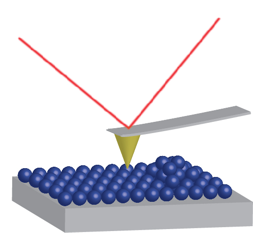
In Atomic Force Microscopy the deflection of a cantilever is measured as a sharp silicon nitride tip is scanned across the sample surface. The tip is held within a few nanometers of the sample surface and the cantilever is bent due to van der Waals forces between the tip and the surface. This bending is detected by a following the position of a laser beam focused at the end of the cantilever using a position sensitive detector. From this, a topographical image of the sample is obtained. The AFM system is capable of imaging surface topography features from a few angstroms to 100 microns.
The AFM system is also capable of imaging the topography using tapping and non-contact modes. In these modes, pure silicon is the tip material and the cantilever is oscillating at its resonance frequency. As the tip approaches the sample surface, the amplitude and the resonance frequency change drastically. This provides the feedback to the scanner. Imaging in tapping mode may be advantageous since it eliminates adhesion and "scratching" effects of soft samples. Imaging under a liquid medium is possible for both the contact and non-contact/tapping modes using a special cell.
Scanning Tunneling Microscopy: A special head is available for using the instrument as a scanning tunneling microscope (STM). In STM mode, a very sharp Pt or Pr/Ir tip is used as a probe. The sample must either be a good conductor or a semiconductor. A bias voltage is applied between the tip and the sample. As the tip approaches within a very short distance of the sample surface, electrons from the tip tunnel through the gap and reach the sample surface. This tunneling current is used to provide the feedback to the scanner. Since more than 90% of the tunneling current comes from a single atom from the tip, atomic resolution is achieved in STM. In addition to imaging the surface, the current-voltage characteristics can also be studied.
X-ray Diffraction (XRD)
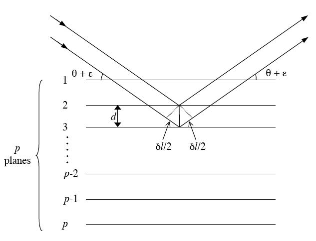
Figure. Schematic representation of x-ray diffraction occuring in a crystal having p atomic planes parallel to the surface with spacing d. In this case the diffraction will follow Bragg's law and the maximum amplitude of the diffracted ray will occur when the path difference, δ, is a multiple of the X-ray wavelength.
X-ray diffraction (XRD) is an important structural technique for characterization of crystalline materials including nanocrystals. This technique provides the crystal structure as well as the lattice parameter of crystals. Apart from providing the structural phase of the nanocrystals, it also provides an estimate of the size of the nanocrystals.
XRD measurements are generally done on solid samples. Generally powered samples are taken on a sample holder. If the sample thickness is too small, the amount of diffracted signal is very small. The most common X-Ray source is Cu Kα with a wavelength (λ) of 1.54 Å. In modern instruments, the detector is a wide-angle detector facilitates acquiring good signal over small period of time.
Considering an ideal crystal having p atomic (hkl) planes parallel to the surface, with spacing d, the approximate thickness of the crystal is close to pd. The amplitude of a diffracted ray will be maximum when the path difference between the rays, δ, reflected from successive planes is equal to a multiple of the wavelength:
This is also known as Bragg's law. The above equation can also be related to the Miller indices by the following equation:
λ is the wavelength (1.54 Å for Cu Kα) and a is the lattice parameter for cubic structure material. One can also determine the minimum crystalline sizes from the broadening of peaks at a specific angle. The Scherrer equation allows the sizes of the crystal faces to be determined using the full width at half maxima (FWHM) of the corresponding diffraction peak. This equation is reliable up to crystallite sizes below 100 nm.

β is FWHM in radians, θ is the Bragg angle and τ is the crystallite domain size.
Energy Dispersive X-ray Spectroscopy (EDX)
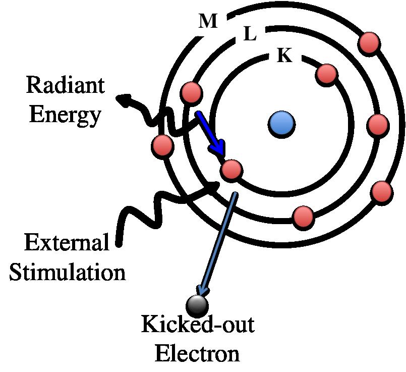
If a sample is excited under high energy of electron beam or other electromagnetic radiation, the inner shell of electrons is ejected to vacuum creating a vacancy in that shell as shown in the following figure. Electrons from the outer shell jump into the vacant site for filling the inner shell. During this process, the sample fluoresces X-ray of energy same as the energy difference between the initial state and final state. Since each atom has its unique and discretized energy levels, the x-Ray fluorescence is also characteristic of that atom. Energy dispersive X ray spectroscopy is a technique that detects the x-ray fluorescence to characterize the elements present in a material.
EDX is typically found as an attachment on Scanning Electron Microscope (SEM) and Transmission Electron Microscope (TEM), where a high energy electron sources are already present. This technique is limited to elements above atomic number 4. Ne needs to be careful while analyzing the data, as several atoms have overlapping peaks at a particular energy. Sometimes, peaks arise due to secondary fluorescence of the sample holder or from the microscope components.
Figure. Schematic diagram of Energy Dispersive X-ray spectroscopy (EDX). In EDX, in incoming X-ray ejects an inner shell electron, leaving a vacancy which is filled by an outer shell electron, releasing a photon.
SiLi detectors operating at LN2 temperature are commonly used in EDX experiments. X-Ray striking the detector produces photoelectrons which in turn produces electron-hole pairs within the Si. These migrate to opposite ends of the detectors (via an applied electric field of 1.5 kV) producing a current pulse whose size is proportional to the energy of the incident X-Ray.
Gas Chromatography/Mass Spectrometry (GC/MS)
In a GC/MS system, gas chromatography is used to resolve gasses and liquids into their individual components which can then be identified using mass spectrometry. This allows for the quantitative analysis of the components in complex mixtures. Our gas chromatograph / mass spectrometer is a new system from Thermo Scientific. The Gas chromatograph has two split/splitless injection ports and one gas sampling valve, and can measure a wide range of samples using either a TCD or a combination ECD/FID system. This enables us to measure gases evolved from photolysis of water or CO2 reduction experiments with high clarity. The mass spectrometer utilizes a single quadrupole and can measure mass-to-charge ratios from 1.2 to 1100. The system also features an autosampler that can handle up to 105 samples and is capable of washing between sample injections to minimize sample crossover. The software includes a NIST library of thousands of compounds to compare samples to.